
Each side of the board will require its own pass down the smd soldering line, so placing all smds on one side will help you avoid some extra assembly costs. Many freeware and open source design programs force you to do everything manually, but advanced pcb design programs like altium designer can help you stay productive as you work to complete your pcb layout and route.

FMEA Risk Assessment for PCB Component Selection
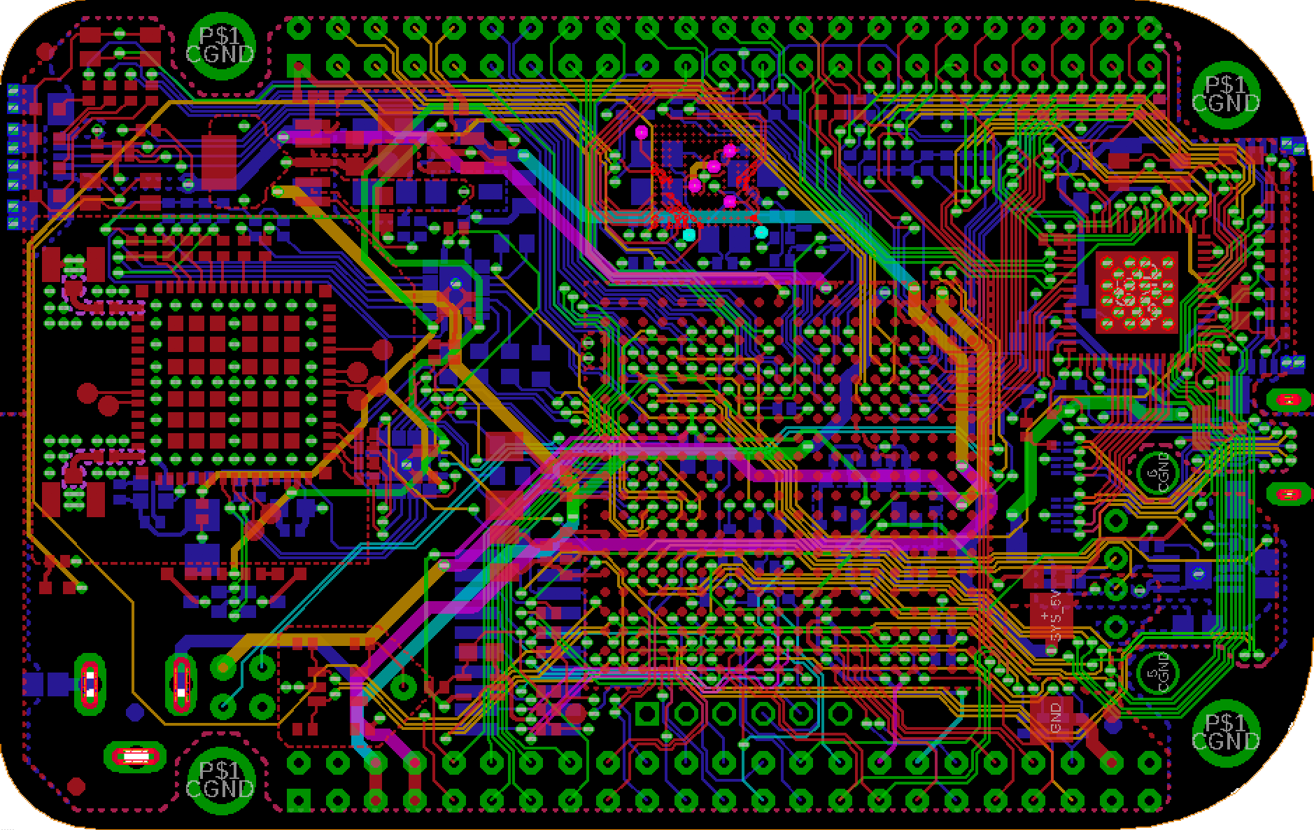
Find the complete course at:
Advanced pcb design rules. Nowadays, a printed circuit board of any modern electronic device should meet the requirements of technologically advanced solutions. It's recommended to place all surface mount device (smd) components on the same side of the board. That is why high speed and high frequency pcb design has become a hot topic for hardware engineering professionals.
For the same reason, prototyping of our circuit boards is very fast. This means the annular ring (radius of the pad) should be at least.005 for vias and a minimum of 0.007 for component holes. Magic leap inc, is seeking a printed circuit board engineer with experience in all phases of pcb design.
As a result, pcb design rules and production processes have evolved to achieve new layouts and capabilities. Bga device design rules www.xilinx.com 5 ug1099 (v1.0) march 1, 2016 chapter 1 general bga and pcb layout overview introduction xilinx® ultrascale™ architecture, 7 series, and 6 series devices come in a variety of The recent advances in pcb design systems and technology have had sweeping effects across the industry.
This allows us to get exceptional pricing and service, especially when it comes to the assembly of pc boards. The pcb milling machine is used to create custom circuit boards for sensors and remote samplers. Components should be arranged in the optimum position for short and direct trace routing.
The circuit board is designed on pcb design software and then can be milled in minutes in the lab. The main reason for this arises during assembly; Once set up correctly, the design rules will automatically select the correct via for the net being routed, easing the designer's workload.
Pad size should be at least + 0.010 over finished hole size for vias and + 0.014 over finished hole size for component holes. Choose reference points that suit the manufacturing process. Board constraint pcb design guidelines.
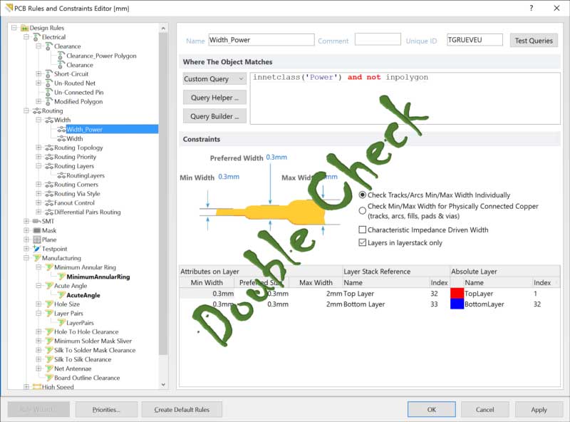
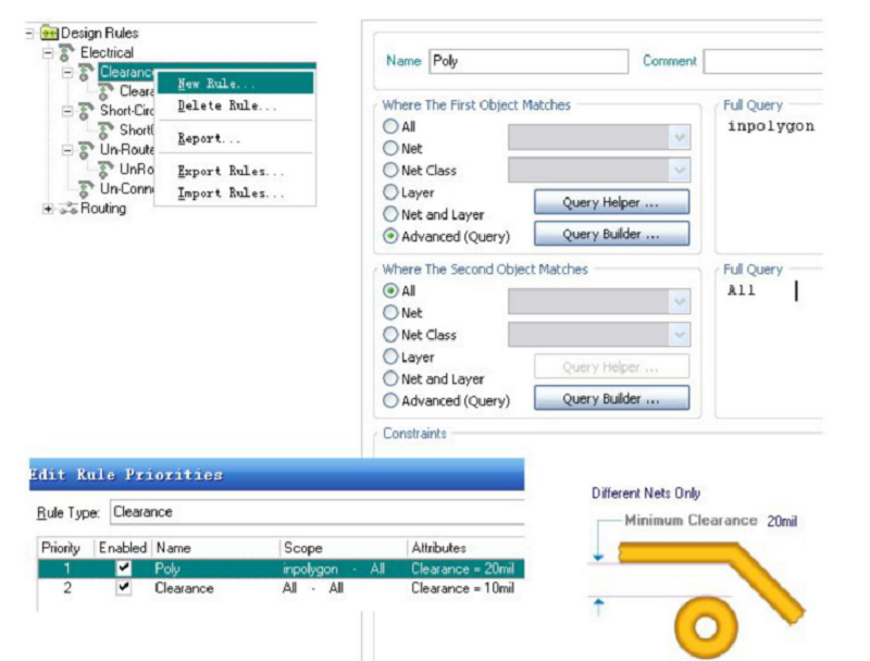
The pcb via design rules allow the designer to manage the different vias that will be used in the design without having to manually change vias for each new net. Design rule checking is a major step during physical verification signoff on the design, which also involves lvs (layout versus. The candidate must have proven experience with product cost reduction while maintaining project timelines.
These should be some of the first factors to be addressed. Taiwan, korea, mexico and china. Pcb design layout guidelines for routing.
This course covers all the important subjects you need to know for advanced pcb layout: It is essential for circuit board designers to layout their board to create the best signal and power integrity possible. Here is where the ability of pcb design systems to communicate directly with the vendor for exchange stackup information, as shown in the video above, can be so helpful.
5 most common high speed design rules. If there is a poor (i.e. Effective component placement will lead to the best trace routing.
Advanced devices will use many more layers. Ideally this candidate will have worked with a broad range of different engineering team. Has developed close relationships with pcb manufacturers and several small and large electronic assemblers and other contract manufacturers, both domestic and offshore.
In this type of routing, the design rules for your nets and groups of nets are checked automatically as you create your pcb layout. Pcb design systems typically have a very comprehensive set of design rules and constraints that can be set up for the design. • most important step in designing a pcb • intelligent placement makes routing easy • typically can place circuit in "blocks" • keep components close together (shorter traces typically are better) • keep power dissipation in mind (spacing/trace widths) • clearance for connectors • separate "noisy" and "quiet" signals
Standard circuit board designs will already be. Design rule checking or check (s) (drc) is the area of electronic design automation that determines whether the physical layout of a particular chip layout satisfies a series of recommended parameters called design rules.

Pcie Pcb Routing Rules PCB Designs
24. Top 5 PCB Design Guidelines Every PCB Designer Needs

Online Advanced PCB Layout Course, by Motherboard Designer
Online Advanced PCB Layout Course, by Motherboard Designer

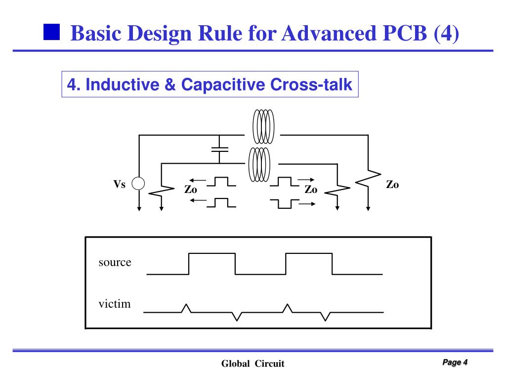
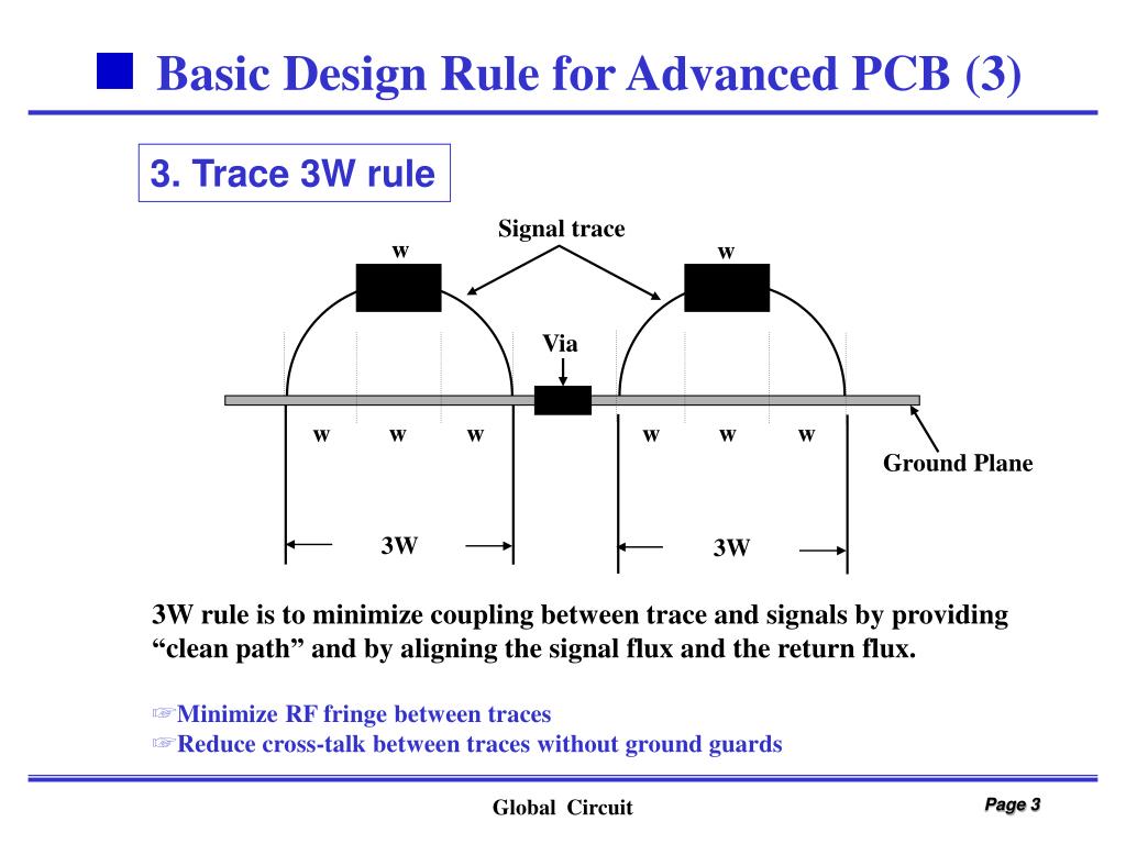
Electronic Board Design Methods based on signal integrity

PCB Advanced Spacing Rules on Altium designer
Online Advanced PCB Layout Course, by Motherboard Designer

![]()
Pcb Spacing Rules Voltage PCB Designs

Basic rules of the PCB design. Download Scientific Diagram

Advanced PCB Layout Course by Fedevel Academy
PPT Basic Design Rule for Advanced PCB (1) PowerPoint
PPT Basic Design Rule for Advanced PCB (1) PowerPoint
Electronic Engineering Capabilities

Advanced PCB Layout Altium

High Speed Routing Guidelines for Advanced PCBs PCB

PPT Basic Design Rule for Advanced PCB (1) PowerPoint
How to Successfully Design a BGA PCB Design Blog
Advanced PCB Layout Step by Step Welldone Blog FEDEVEL


Pcb Layout And Pcb Design PCB Circuits